

 MENU
MENU
Imagica Technology, Inc. designs and manufactures high-performance image sensors that utilize technology licensed from Lumiense Photonics and from a variety of CMOS and scientific photodiode fabrication processes.
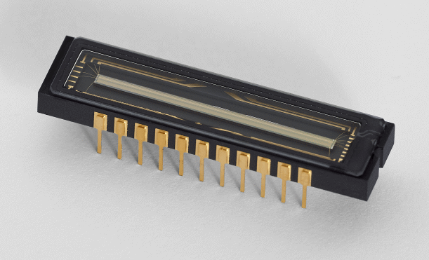
When Sony Semiconductor discontinued their ILX linear image sensors Imagica invented a series of line scan sensors designed specifically to replace several of those as initial product line. The ITR series will all be available with taped-on windows for users who need to apply special windows or to coat the sensor directly – no window removing needed. The first two of these sensors, the ITR-511, a replacement for the Sony ILX511B and the ITR-554 as a substitute for the Sony ILX554B, are now available.
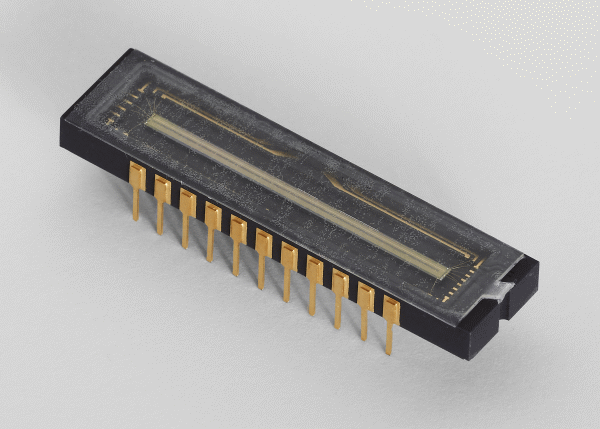
The Imagica Technology ITR-511 is a high performance CMOS linear image sensor with 2048 pixels. It can be used as a socket-compatible replacement for the Sony ILX511B CCD linear sensor. Advanced CMOS technology is used to emulate the signal level scheme of the ILX511B ensuring both signal level and pin compatibility.

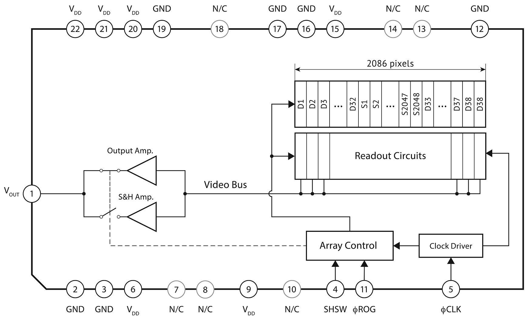
Configuration
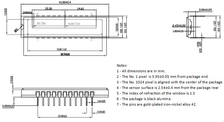
Package dimensions
Are you interested in further details? Download the the manufacturer's full product description.
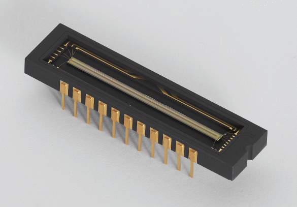
The Imagica Technology ITR-554 is also a high performance CMOS linear image sensor with 2048 pixels. It can be used as a socket-compatible replacement for the Sony ILX554B CCD linear sensor. Advanced CMOS technology is used to emulate the signal level scheme of the ILX554B ensuring both signal level and pin compatibility.
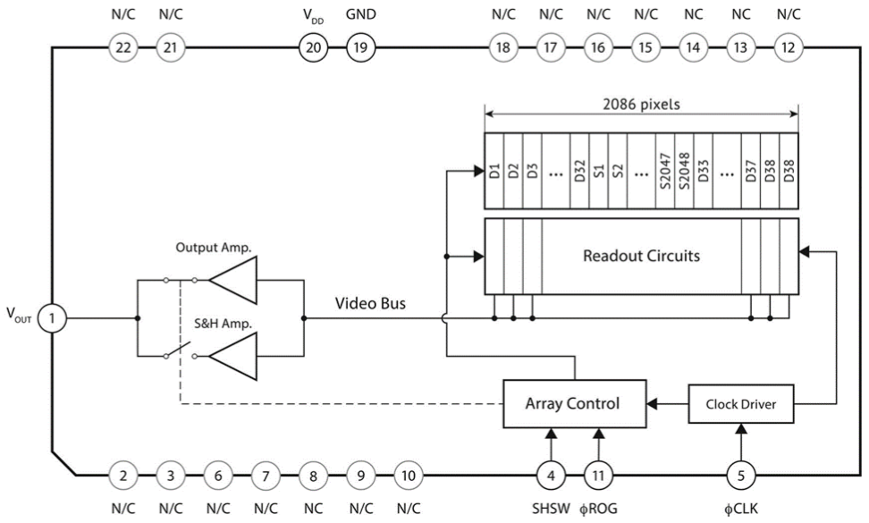
Configuration

Package dimensions
Are you interested in further details? Download the the manufacturer's full product description.
Unlike the Sony sensors, the ITR series will all be available with taped-on windows to easily apply special windows or coating. To remove the taped-on window, just pull on the tape and the temporary window comes off.
Temporary window in place.
Temporary window removed.
Of course, Eureca also offers its expertise in the field of coatings and special coverslips for the Imagica sensors. Please contact us if you have questions or special requests!
Additional models in this line should be available including replacements for the ILX503B, ILX551B, ILX703B ad ILX751B. If you need any of these sensors to sustain your production, please contact us!
Imagica's ITC576A is a high performance CMOS linear sensor for building Contact Image Sensors (CIS). It supports a wide range of resolutions – 1200, 600, 400, 300, 200, 100 dots per inch (dpi) – and operates at up to 40MHz. A Low Voltage Differential Signaling (LVDS) clock interface enables high speed operation and wider module assemblies with lower noise. The ITC576A includes an output amplifier with sample & hold video output, Correlated Double Sampling (CDS) and a global shutter mechanism.
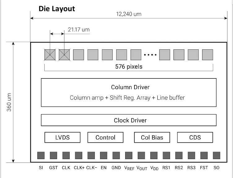
Die Layout.
This device is supplied in lots of slightly more than 5,000 die on a 200mm background wafer in a sealed coin stack container as shown nearby. Users must be experienced in sawing thin wafers and mounting small die.
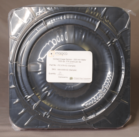
Sealed coin stack container.
Here you can easily ask a question or inquiry about our products:
Last update: 2019-05-02

EURECA Messtechnik GmbH
Deutz-Kalker Straße 35, D-50679 Köln
![]()
![]() Phone: +49 (0)221 952629-0
Phone: +49 (0)221 952629-0
Fax: +49 (0)221 952629-9
info(at)eureca.de
www.eureca.de


