

 MENU
MENU
With integrated circuits in BGA package, the SMD connectors are aligned compact at the bottom of the component. This type of housing is mainly used for complex components with many connections.
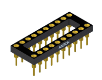
An elongated housing for electronic components, where there are two rows of pins on opposite sides of the housing. For a long time, this was one of the most common design for integrated circuits, but even today there are a number of components that use this package.
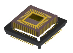
A package with J-shaped inward-curved SMD connectors, which was originally commonly used for flash memory, but is today also used for e.g. image sensors.
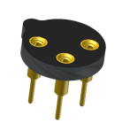
In addition to transistors this package is used by many other classes of electronic devices, such as laser diodes, gas sensors and much more.
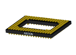
In this package form, the individual contacts are arranged in a grid. In addition to rectangular and square designs, there are also types in which the interior of the component is free.
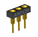
Rows of contacts with different numbers. In addition to the long time mainly used grid size of 2.54mm, other grid dimensions are available.
Here you can easily ask a question or inquiry about our products:
Last update: 2018-11-21

EURECA Messtechnik GmbH
Deutz-Kalker Straße 35, D-50679 Köln
![]()
![]() Phone: +49 (0)221 952629-0
Phone: +49 (0)221 952629-0
Fax: +49 (0)221 952629-9
info(at)eureca.de
www.eureca.de


